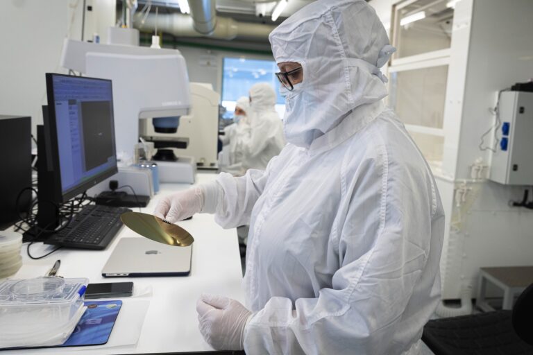
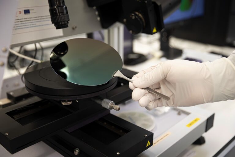
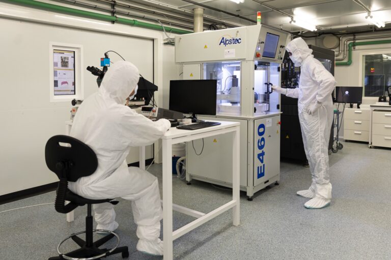
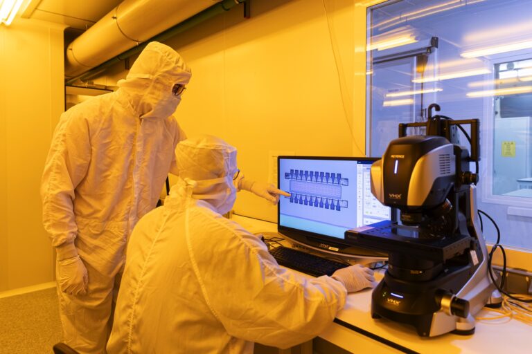
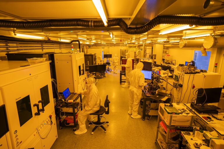
500 m² of ISO-7 cleanroom space and automation tools for semiconductor backend processing at Universitat Politècnica de València.
ISO-7 Cleanroomas
0m2
Research Institutes
0
Class Rating
0k
Our focus
Photonic Integration
Hybrid integration of photonic chips using advanced flip-chip bonding and silicon nitride waveguide platforms.
Semiconductor Processing
Full backend processing of semiconductor wafers with ISO-7 grade deposition, lithography, and etching.
Packaging & Assembly
Automated tools for die attach, wire bonding, and encapsulation services for photonic and electronic chips.
R&D Access
Open access to equipment and process expertise for universities, institutes, and industrial partners.
Resident Programme
Co-location of companies within UPVfab facilities with shared infrastructure and technical support.
Technology Transfer
Bridging academic research and industrial deployment through pilot line validation and process transfer.
Our ecosystem
We are the result of the joint work of UPV research institutes specialised in photonics, chemistry and electronics, bringing together expertise to drive innovation in deep tech and semiconductor technologies.